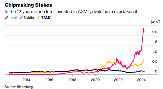
It was a strategic misstep of epic proportions. The US took a crucial early role in developing the semiconductor technology that underpins today’s revolution in artificial intelligence. Yet it’s a Dutch firm that now holds a monopoly on the process, and Asian manufacturers that dominate production.
Extreme ultraviolet lithography machines are arguably the most significant electronic devices in the world right now. Their arrival has enabled the assembly of chips offering a step-change in processing power, paving the way for a new generation of AI tools. The vast and multi-level computation performed by AI platforms such as OpenAI’s ChatGPT and Google’s Gemini accelerates a multitude of tasks usually performed by humans. That’s made access to EUV technology a matter of national economic security for the US and China.
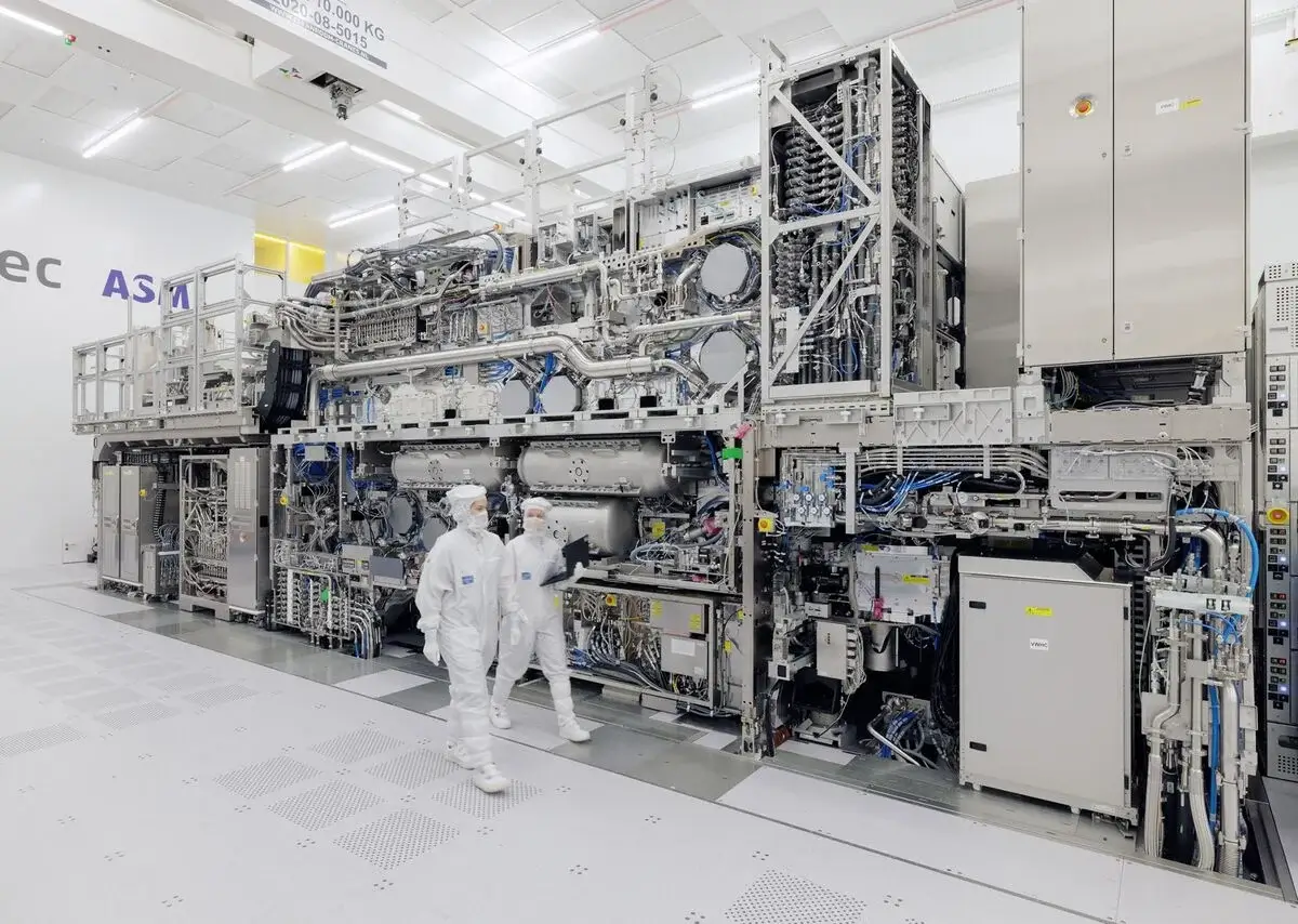
The problem for Washington, and Beijing, is that EUV machines are made by just one company: ASML Holding NV. Each device is the size of a bus and costs more than $200 million apiece. More than 200 have been shipped so far, turning ASML into Europe’s most valuable tech stock, with a market capitalization topping $350 billion.
How did the US manage to cede control of this crucial technology? Part of the reason is that relatively few industry executives ever thought that EUV could work. Another cause: misjudgments by what was for a long time the world’s biggest chipmaker, Intel Corp.
Near-Atomic Scale
Silicon chips consist of transistors – essentially a series of gates and switches that are the physical manifestation of the zeros and ones of modern-day computing. To make computers more powerful, semiconductor engineers are in a constant quest to make transistors smaller. The first that were invented in the middle of the last century were about a centimeter long. Now, they’re just a few nanometers across, or several billionths of a meter.
In the first few decades of chipmaking, visible light was used to burn patterns into the silicon to create the transistors – a process known as lithography – before the industry then migrated to ultraviolet light. In the 1980s, scientists started to wonder how chipmaking might get to the near-atomic scale that would be required to maintain the pace of innovation. Researchers at New Jersey-based Bell Labs started looking into extreme ultraviolet technology, followed by three of the Department of Energy’s national laboratories: Lawrence Livermore, Lawrence Berkeley and Sandia. The DoE ended up putting tens of millions of dollars into the research.
As those institutions made progress on some of the technical elements, they realized that industry backing would be essential to bring it to market. A public-private partnership dubbed EUV LLC was formed in 1997, bringing on board US companies Intel, Advanced Micro Devices Inc. and Motorola Inc. It ultimately expanded to include the lithography firms Silicon Valley Group Inc. and ASML, which was also involved in a similar EUV research consortium in Europe.